Tutorials

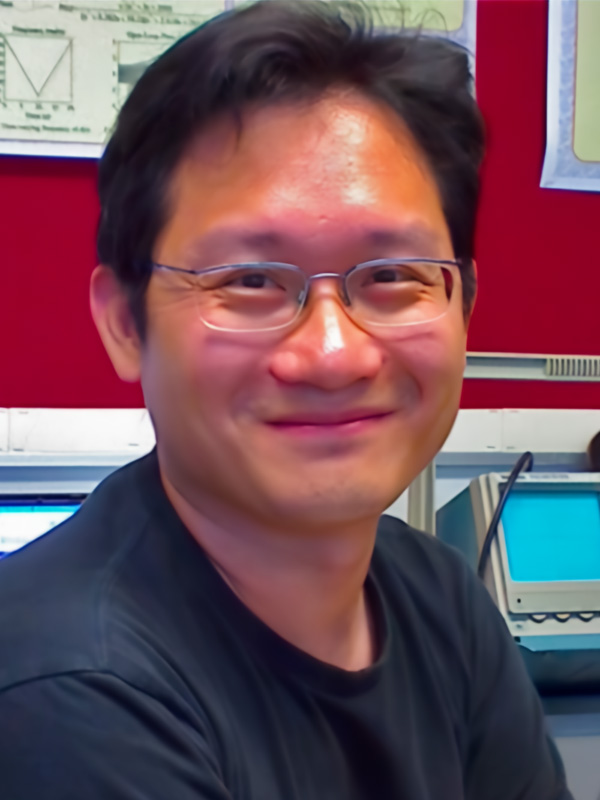
Hsin Liang Chen
Tutorial 1

Digitally-Assisted Auto-Calibration Techniques for Analog and Mixed-Signal Circuits Against PVT and Environmental Variations

Dr. Hsin-Liang Chen

Assistant Professor
Tamkang University, Taiwan

Wednesday, September 9, 2026 16:00-16:30 Wah Lee Hall, 1F, Building of International Research

Abstract

This tutorial presents digitally-assisted auto-calibration techniques to mitigate process, voltage, and temperature (PVT) variations in analog and mixed-signal integrated circuits. Rather than relying on expensive multi-point post-fabrication trimming, the discussed architectures leverage on-chip sensing and digital search algorithms to implement robust self-healing mechanisms. Three silicon-proven designs demonstrate this paradigm across different circuit levels. First, a 25-μA reference current source fabricated in standard 0.18-μm CMOS employs a current-controlled ring oscillator and a 7-bit binary search controller, achieving a low temperature coefficient of 206 ppm/°C across an extreme range of −40°C to +115°C. Second, an integrator RC time-constant calibration scheme in TSMC 90-nm CMOS uses a modified 10-bit voltage-to-digital converter with a self-calibrating dynamic comparator, reducing time-constant errors from ±20% to about 1%. Third, a 6th-order Gm-C bandpass filter for capacitive touch sensing utilizes an auxiliary Gm-C LC oscillator to execute a fast 12-ms 6-bit binary search, aligning the center frequency to 200 kHz with a post-calibration frequency offset of just 2.1%. Collectively, these methodologies exhibit low-power, compact, and highly scalable solutions essential for modern resilient microelectronics.

Biography

Hsin-Liang Chen received the B.S., M.S., and Ph.D. degrees in electrical engineering from Tamkang University, Taipei, Taiwan, in 1999, 2003, and 2009, respectively. From 2010 to 2014, he worked as an Analog Circuit Design Engineer at the Industrial Technology Research Institute (ITRI), where he designed high-speed analog-to-digital converters (ADCs). From 2014 to 2016, he was a Senior Analog Circuit Design Engineer at Weida Hi-Tech, where he worked on developing touch-panel controller ICs. From 2017 to 2023, he was an Assistant Professor in the Department of Electrical Engineering at Chinese Culture University, Taipei, Taiwan. In February 2024, he joined the Department of Electrical and Computer Engineering, Tamkang University, where he is currently a faculty member. His research interests include mixed-signal CMOS integrated circuits, delta-sigma ADCs, high-speed ADCs, and low-power analog circuit design.

Dr. S. Malavizhi
Tutorial 2

Machine Learning Algorithms for VLSI Design

Dr. S. Malarvizhi

Professor
SRM Institute of Science and Technology, India

Wednesday, September 9, 2026 16:30-17:00 Wah Lee Hall, 1F, Building of International Research

Abstract

Machine learning and deep learning techniques are increasingly embedded across the entire VLSI design pipeline, spanning specification, RTL coding, verification, logic synthesis, physical implementation, manufacturing test, and tape-out. Historically, this pipeline has relied on rule-based, heuristic-driven Electronic Design Automation (EDA) tools — simulated annealing for placement, deterministic synthesis compilers, exhaustive Design Rule Checking, and exhaustive fault simulation for test — all of which scale poorly as chip complexity grows into the billions-of-transistors regime dictated by continued technology scaling. This computational and time-to-market pressure has motivated a shift toward data-driven, predictive, and generative models that either augment or directly replace these heuristic stages.

Complexity outpacing tool scalability,NP-hard spatial optimization,Prohibitive simulation and test cost,Late discovery of failures relative to signoff criteria- these pressures motivate ML in chip design industry.but the biggest challenge is in Adopting ML for VLSI Design is Data Scarcity: High-quality labeled datasets are often limited in availability, hindering ML model training. This session through an insight of basic ML algorithms in classification, regression , GNN for predicting delay, autoencoders for test pattern classification and need of transfer learning in VLSI.

Biography

S. Malarvizhi obtained her PhD degree in wireless communication from College of Engineering , Gunidy Anna University in 2006. She is working as a Professor in the Department of ECE, SRMIST, Kattankulathur, Chennai. She received research grant from Board of Research in Nuclear Science, Department of atomic energy ,Government of India- BRNS for the project titled: Real Time Hardware Based Raw Data Processing for Dual Energy X-ray Baggage Inspection Systems (XBIS) for the Detection of Hazardous Materials”,Sanction number:34/14/07/2017-BRNS/34282. Received Women In technology WIT Xilinx award 2021 from Xilinx( presently AMD) for development of the ML algorithm in PYNQ -Z2 board for early diagnosis of breast cancer diagnosis. She also received grant from DST(Department of Science and Technology , Government of India) to develop a prototype for “Development of an loT enabled surveillance system for monitoring falls and medical emergencies of senior citizens living independently”

IEEE India Council awarded her as women innovator for the year 2025 - for contribution in technology. IEEE-Madras chapter has been recognized twice for her contribution in publication and research above age 50. She has 2 granted patents and nearly 40 SCI publications.